ContentsDisclaimerRedistribution and use of this article or any images and files referenced in it, in source and binary forms, with or without modification, are permitted, provided that the following conditions are met: - Redistribution of article must retain the above copyright notice, this list of conditions, link to this page and the following disclaimer.
- Redistribution of files in binary or source form must reproduce the above copyright notice, this list of conditions, link to this page, and the following disclaimer in the documentation and/or other materials provided with the distribution, for example, Readme file.
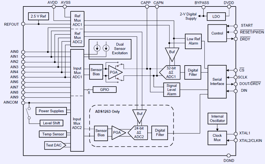
All information posted here is hosted just for education purposes and provided AS IS. In no event shall the author, element14, or any other 3rd party be liable for any special, direct, indirect, or consequential damages or any damages whatsoever resulting from loss of use, data or profits, whether in an action of contract, negligence or other tortuous action, arising out of or in connection with the use or performance of information published here. IntroAnalog-to-digital converters are electronic devices used to measure analog world values and convert them into digital code, which can be processed by digital processors and computers. Usually input signal is related to voltage, which is converted into code by various ADC topology methods. Many applications today, be it industrial controller or smartphone have number of ADCs integrated, providing way to interface with sensors. This allows data like voltage, current, temperature, pressure, humidity and many others to be processed by digital controllers and building responsive system. There are many different ADC types. For most of use cases ADC blocks integrated in micro-controllers and SOC are already good enough. These are cheap, easy to interface and does not take space on PCB, it’s almost free additive of digital ASICs. Still, in some other areas, much higher precision or higher speed is required, making use of separate discrete ADC chips viable. In the past, an ADC providing 8 or 10-bit resolution was good to measure almost any signals. Standalone Δ-Σ ADCs are usually best choice to do low-speed high-precision measurements, providing required accuracy and resolution. This type ADC often can come with stable integrated voltage references, PGA and current sources for various sensor applications. Resolution for most ICs is in 16-24 bits range, with very good noise and DC performance. In this review new greatest solution in data converter world, 32-bit Δ-Σ ADC from Texas Instruments is covered and tested, using ADS1262 evaluation kit package. This kit was received from element14’s RoadTest program and will be evaluated thru some possible scenarios of use. This is a starter platform, relatively affordable for most hobbyists and instrumentation professionals, who looking into high-precision measurements. This is first article in series, with introduction to kit, overview of market offerings for ultra-high 32-bit resolution analog to digital converters, construction features and usage approach for TI ADS1262EVM-PDK. We will briefly compare specs of highest resolution ADC from TI and competitors and get ready with set of practical experiments to test performance of this 32-bit ADC. Worth to mention, that some parameters of such high-precision device would be extremely hard to test without expensive specialized equipment. I’ll put my best effort to ensure accuracy and usability of obtained results. To aid this task multiple high-performance bench DMMs and sources will be used. If we think for a second, 1 LSB of 32-bit A/D output of 2.5VDC full-scale signal is equal to 0.581 nanovolts (2.5 / 232). This is far-far down in the levels of thermal noise in practical circuit. Compare this to 2.4 mV LSB in “usual” 10-bit ADC system! 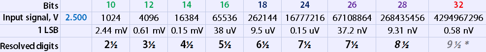
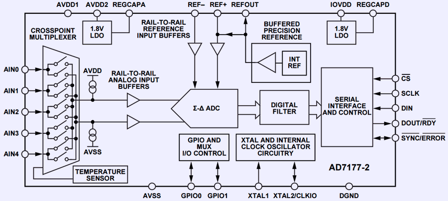
Table 1: Resolution versus resolved voltageResolution over 24 bits in past were only achievable by expensive and complex multislope integrating discrete ADCs (used almost in every 6½-digit+ DMM). For example, industry standard long-scale 8½-digit HP 3458A provide 28-bit conversion data from it’s $1300 USD worth custom integrating A/D converter, with help of trimmed ultrastable resistor networks, proprietary semiconductor tech and fast logic. Theoretical limits are shown above are based on ideal ADC case, which is not a quite accurate with respect of real-world devices and physics. Down at this level of resolution thermal effects, matching inaccuracy, noise pickup from surrounding circuits and fields limiting performance to much lower levels. It’s not like you can buy one of these ADC’s, connect usual voltage reference from the shelf and get good 8½-digit readings. Due to practical issues of having so wide dynamic range digitizing capability require lot of design effort. Careful design must be done to achieve even 5½-digit stable results. Some of these issues would be covered and discussed later, some are not, but these are some of reasons why there are only a few 7½-digit and 8½-digit instruments exist, and all of them are using slow and expensive discrete integrating A/D converters. There are no unimportant detail when it comes to precision analog design. Having all this said, does it make 32-bit ADC useless? Let’s test and see! High-resolution ADC comparisonAs of today (November 2015) there are only two vendors can sell 32-bit ADC chip. It’s Texas Instruments which we will study and test later, and Analog Devices. Let’s take a look on what these guys have to offer: | Texas Instruments ADS1262 | | Block diagram (zoomable) | | | ADC Type | 32-bit Δ-Σ | 32-bit Δ-Σ | Output rate | 2.5 SPS to 38.4 kSPS | 5 SPS to 10 kSPS | Channel rate | | 10 kSPS/channel (100 μs settling) | ENOB max speed | 15.6 bits at 38.4 kSPS | 19.1 bits at 10 kSPS | ENOB mid speed | 21.1 bits at 7.2 kSPS | 20.2 bits at 2.5 kSPS | ENOB min speed | 26.0 bits at 2.5 SPS | 24.6 bits at 5 SPS | INL | ±12 ppm of FSR | ±3.5 ppm of FSR | Channels amount | 5 differential or 11 single-ended | 2 fully differential channels or 4 single-ended | Analog input range | ±VREF (AVSS-0.3 < VREF < AVDD+0.3) | ±VREF (AVSS < VREF < AVDD1) | Analog input current | ±2nA (buffered) | ±30nA (buffered) | Input buffers | PGA, 1/2/4/8/16/32 | True rail-to-rail analog and reference | Analog voltage reference | Internal 2.5V or up to 3 external inputs | Internal 2.5 V reference or external | Internal VREF TC | ±6 ppm/°C max | ±5 ppm/°C max | Noise 0.1 Hz to 10 Hz | 0.145μV(RMS) | 4.5μV(RMS) | Clocking | Internal 7.3728 MHz, Ext 8MHz | Internal or external, 16MHz | PSRR,CMRR | PSRR 90dB, CMRR 110dB@60Hz | PSRR 95dB, CMRR 95dB@DC, 120dB@50/60Hz | Power requirements | AVDD = 5V, DVDD = 2.7 to 5V | AVDD1 = 5 V, AVDD2 = IOVDD = 2.5 V to 5 V | Onboard temperature sensor | Yes, 420μV/K | Yes, 470μV/K | Onboard current source | 50/100/250/500/750/1000/1500/2000/2500/3000 μA | 10μA | GPIO | Multiplex with analog inputs | 2, dedicated pin | Temperature range | -40°C to +125°C | -40°C to +105°C | Digital interface | SPI | SPI, QSPI, MICROWIRE, and DSP compatible | MSRP | $9.10 USD | $23.75 USD | Datasheet | | | Eval.board kit cost | | |
Table 2: Specification comparison of 32-bit ADCs TSSOP package is possible to hand solder with little care and wave reflow soldering iron tip. There are also lot of prototype boards available for this packages as well. The ADS1263 IC variant is based on same design, but have additional auxiliary 24-bit Δ-Σ ADC, which can be used for monitoring signal on lower gain, or for compensation/ranging purposes. As shown in functional block diagram, both ADS1262 and ADS1263 feature eleven analog inputs, configurable as ten single-ended inputs, five differential inputs, or any combination. Analog inputs support next functions: Function / operation mode | Pins | | External reference input 1 | AIN0+AIN1 | External reference input 2 | AIN2+AIN3 | External reference input 3 | AIN4+AIN5 | Two current sources for excitation | Any analog input | Level shift (bias to middle supply level) | AINCOM | GPIO mode | AIN3-AIN9, AINCOM | Sensor current source | Any analog input | Test signal output | AIN6, AIN7 |
Table 3: Inputs configuration and related pins After input multiplexer, signal is fed into a high-impedance programmable gain amplifier (PGA). The PGA have low voltage and current noise. Gain can be programmed from 1 V/V to 32 V/V in binary steps. The PGA can be also completely bypassed, to allow the input range to extend below ground level when using single-voltage power supply. PGA also has voltage over-range monitors, to alert user when it’s out of spec conditions. The programmable sensor bias available to use a small test current for detection of a failed sensor or incorrect sensor connection, if this function is used (for example in measuring thermocouples or RTDs). The ADC core operates with the internal +2.500 VDC reference, or with up to three external reference inputs. The external reference inputs are continuously monitored for low or missing voltage. The REFOUT pin provide buffered +2.500 VDC (±10mADC drive capability) internal voltage reference output for monitoring or external analog circuits use. TI also provide handy Excel calculator to aid engineers calculating proper configuration and proper input signal parameters for front end design. 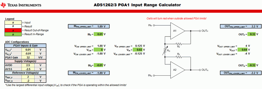
Image 1: TI ADS126X calculation Excel toolkit
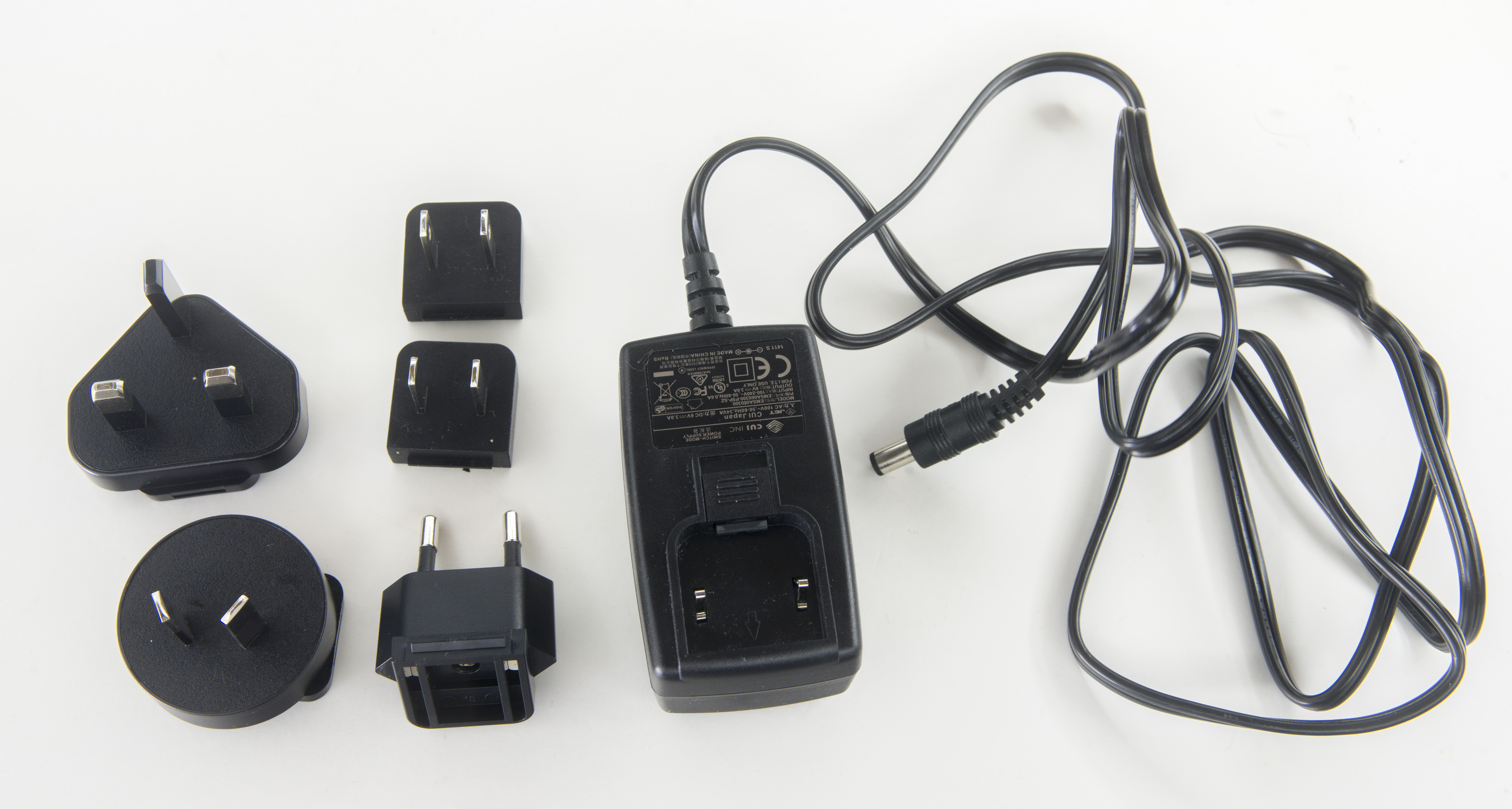
Image 2: EVM package exteriorKit received in rather large box, with lots of packing and protection foam to keep contents safe. There is very little chance that anything will get damaged even with rough shipping services. This could also drive shipping cost bit higher than expected, if shipped internationally. Box contents: - Universal 100-240V mains brick, +6VDC 3.0A output
- Texas Instruments MMB0 Rev.D main interface board
- Texas Instruments ADS126XEVM Rev.A
- Standard USB Type-B cable
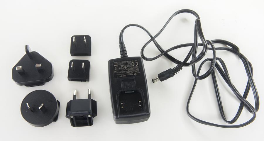
Image 3: Power supply and mains plugs adaptersPower supply having funky interchangeable plugs to fit universal regions, with two exactly same US-type ones. Perhaps one is extra? Taiwan is using same sockets as US, so pretty standard stuff. Before we go into details, it may be worth to mention, TI have another, more specialized evaluation kit for ADS1262/ADS1263 exists, but not available for sale: PDK Hardware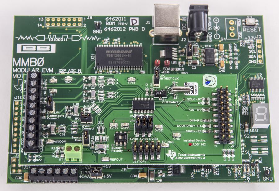
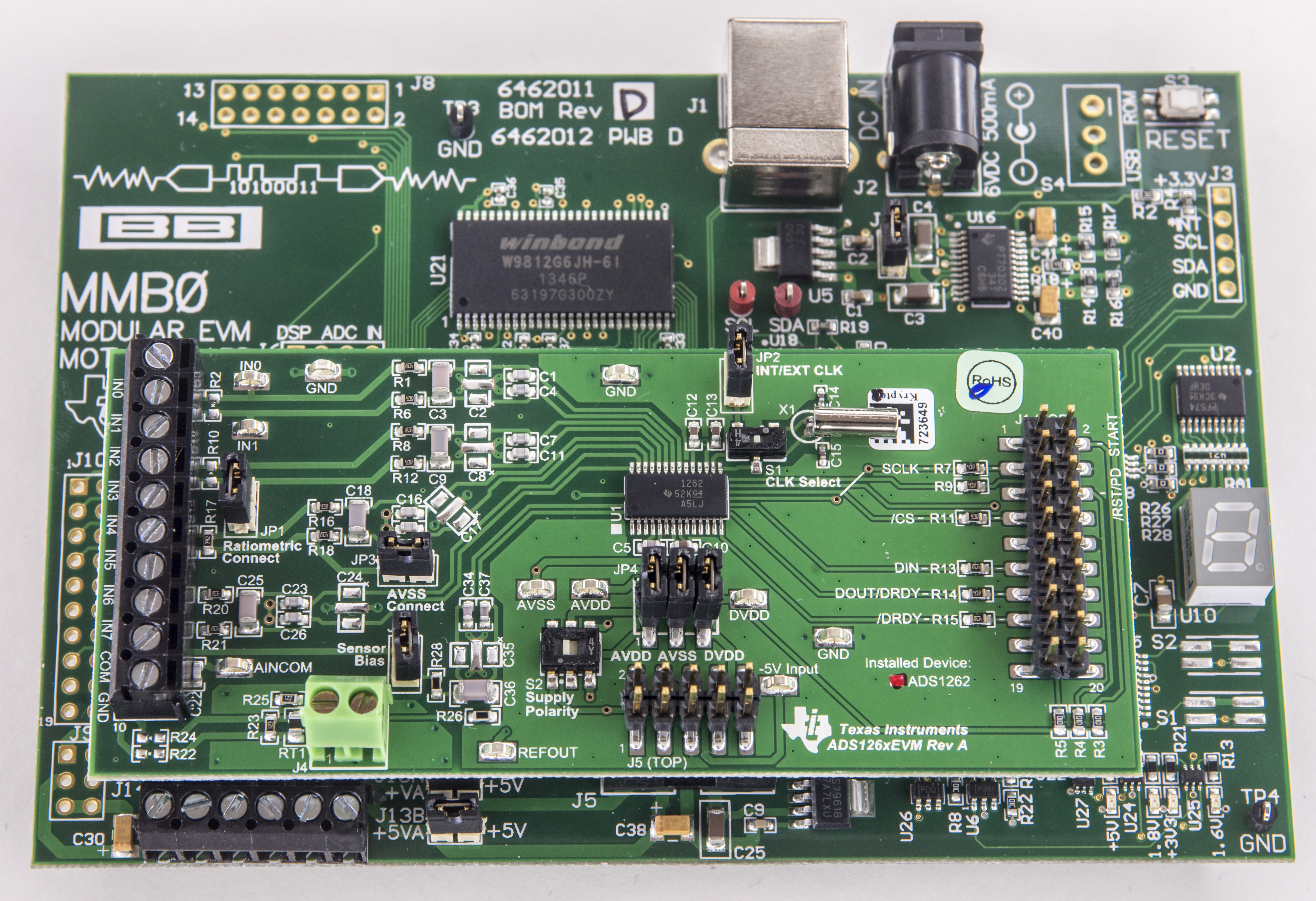
Image 4: Assembled base-board MMB0 and ADS126XEVM module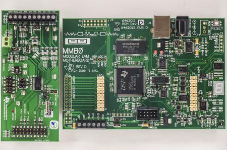 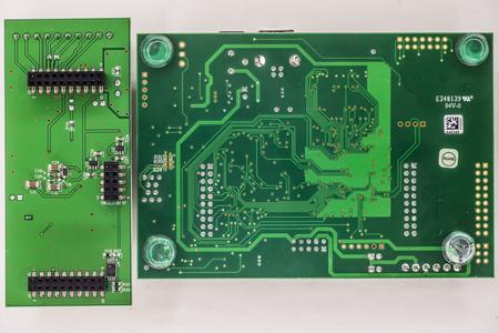
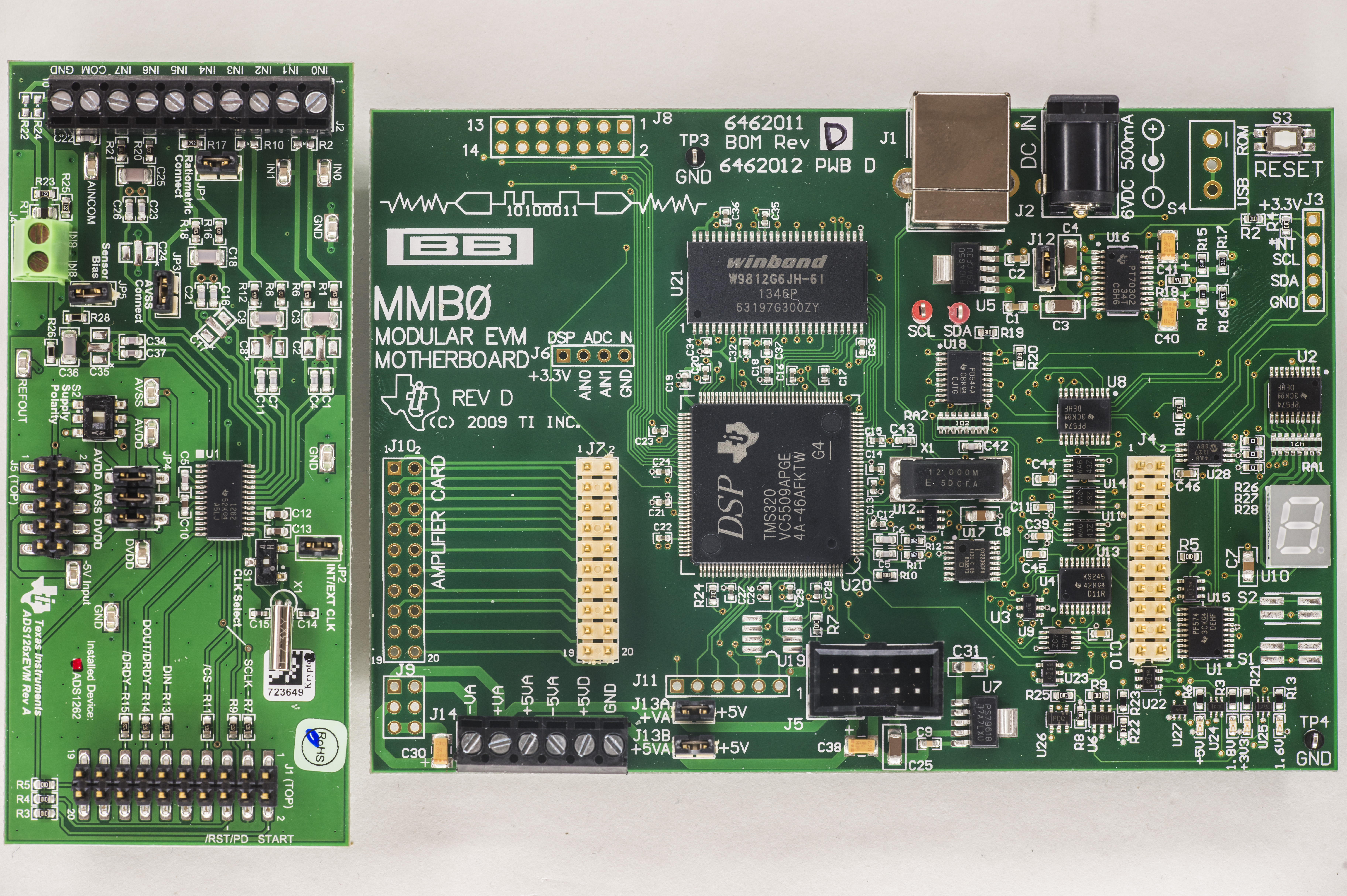
Image 5,6: Boards overview, top and bottom sidesBoth boards are interconnected via three regular pitch 2.54mm pin headers, with digital, analog and power signals routed from main interface MMB0 board. This main board supports various ADC and DAC evaluation modules, so same test environment can be used for every specific application.  
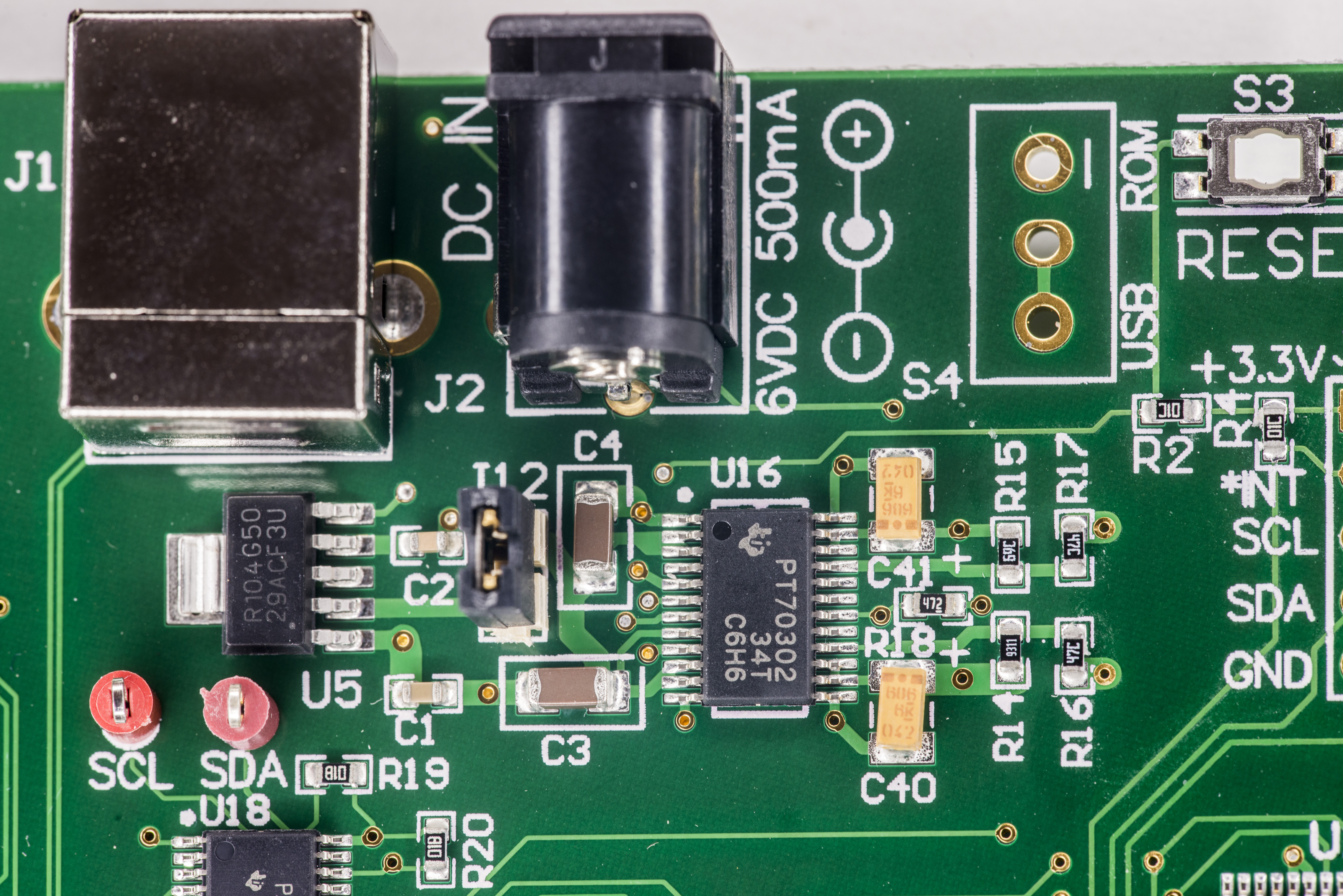
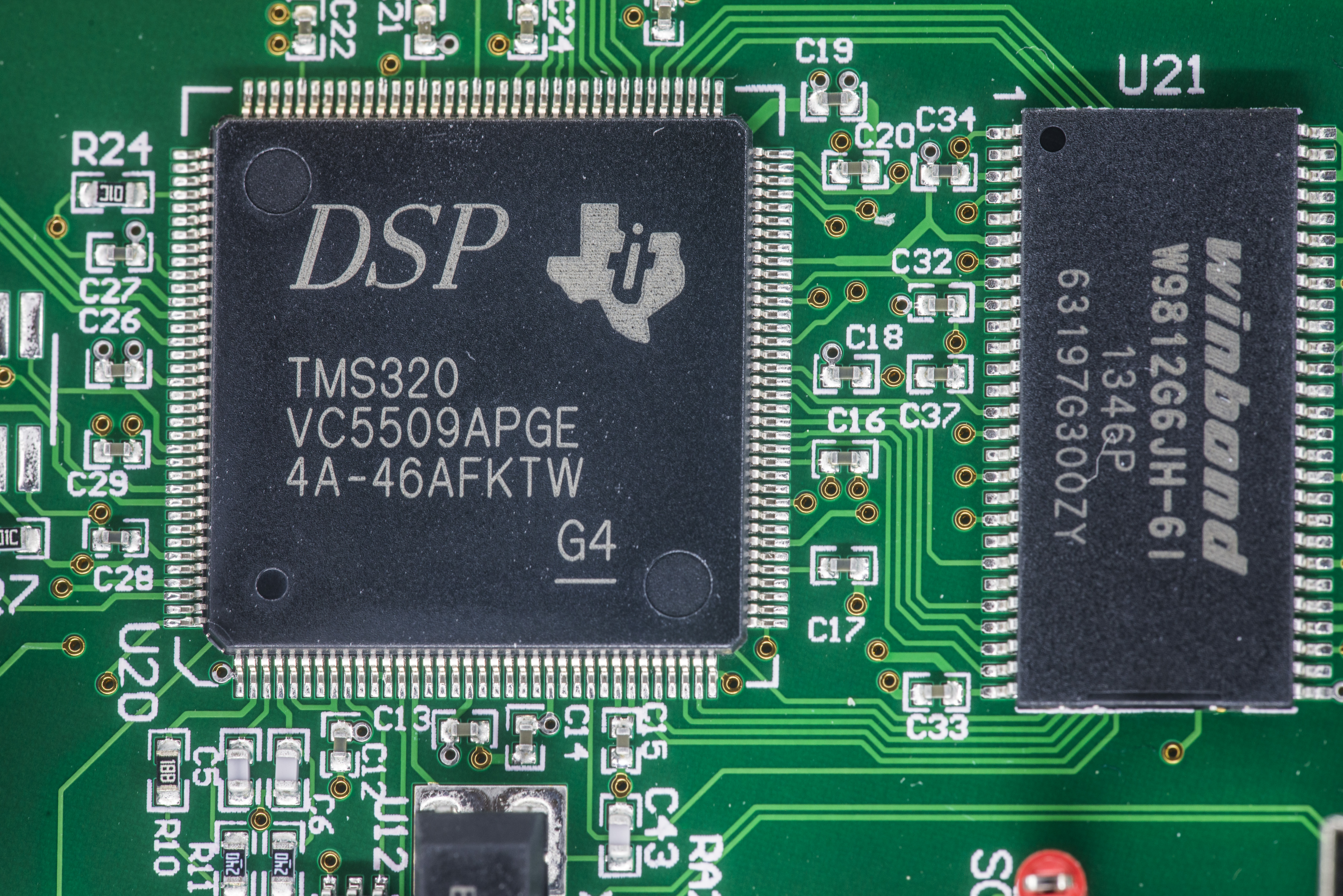
Image 7,8: USB interface, DC power input jack and power status LEDsUSB port is only for digital data connection, and does not carry power to any parts of PDK, so do not expect things to work with just USB cable plugged in. Power delivered from separate DC jack, which accepts +6VDC. Inner pin of DC jack is positive, no surprises here. Use of DC jack instead of USB power is due to requirements of low noise power supply for ADC, to reduce chance of unwanted noise coupling to sensitive ADS1262. Noisy USB power supply from PC can easily upset such 32-bit ADC evaluation kit, so extra care was taken by TI. Onboard TMS320VC5507PGE DSP used only as interfacing bridge, and not doing any math or filtering work. Everything is done on PC software side. This approach have both positive and negative sides, as MMB0 supports many different EVM boards with various ADC and DACs, TI opted for single but versatile design with on-board DSP chip, even if it increase cost of evaluation kits. Some engineers which consider using TMS320 DSP+ADC/DAC may find this useful, as they get both pieces in one package. 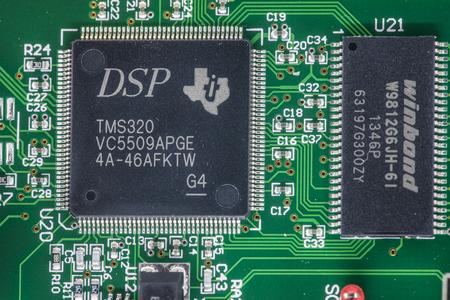 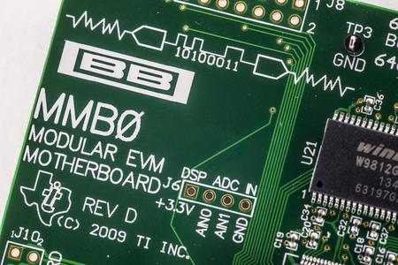
Image 9,10: TI TMS320 DSP and MMB0 logo artworkFew more photos of board powered and ADC module attached: 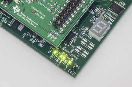 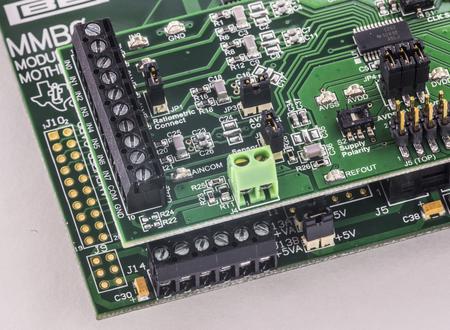
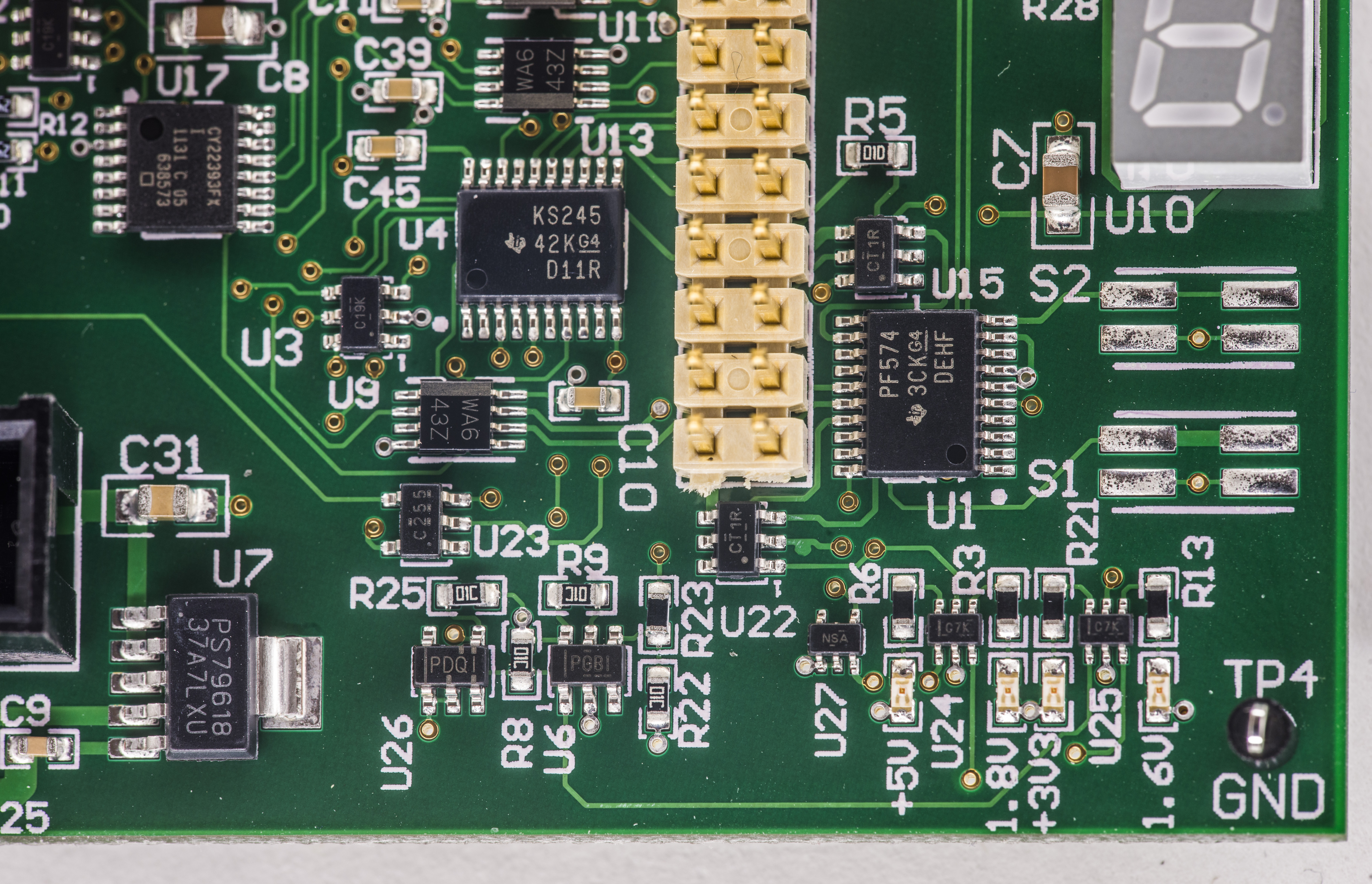
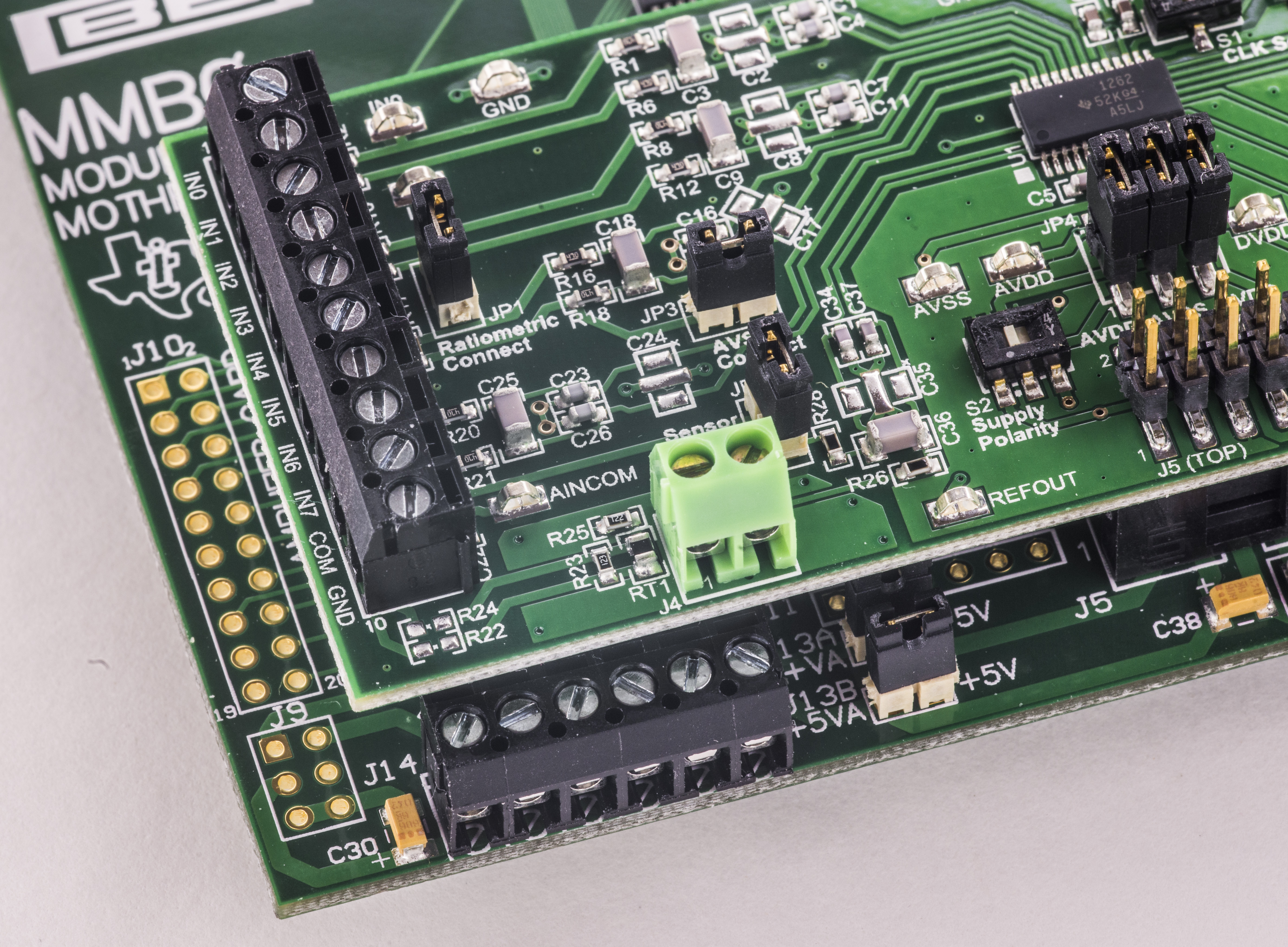
Image 11,12: Power LEDs operation and input signal terminal blocksPower presence status is monitored by four green LEDs in bottom right corner, allowing to quickly determine status and operation of mainboard power supplies. There are no activity or other LEDs except single-digit 7-segment LED. Analog section, ADS126XEVM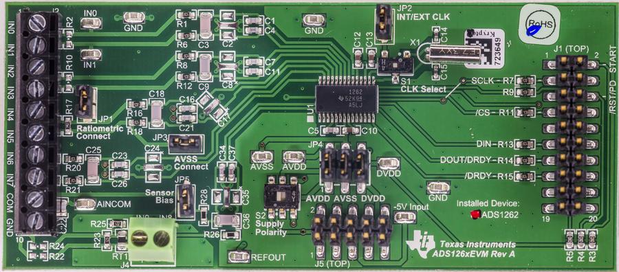
Image 13: ADS126XEVM module, top component sideAdd-on plugin with ADC chip and on-board ±2.5V supplies. It is FR4 4-layer PCB, with good quality and nice silkscreen around all parts and test points. Assembly quality is very good, no bodges or jump wires present. Board also have two switches to set operation mode. Switch location | Function | S1, near crystal | Select between JP2 external clock input or onboard 7MHz crystal X1 | S2, near JP4 | Select single supply +5VDC or dual supply ±2.5VDC operation |
Table 4: Module switch configuration 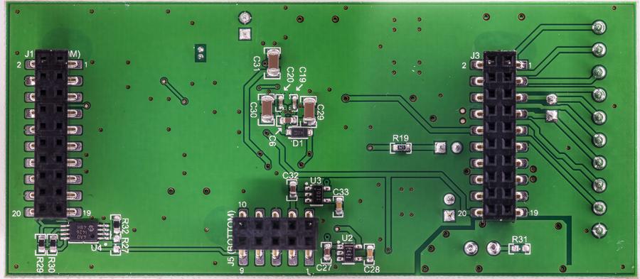
Image 14: ADS126XEVM module, bottom component sideBottom side of PCB have only linear supplies U2, U3 and U4 and some decoupling capacitors and resistors. Pin headers from top duplicated with SMT female headers, so board signals are routed thru. Handy for integration on custom breadboards and test PCBs. PDK SoftwareBundled software is based on NI LabView, including source project files, with all it’s pro’s and con’s. It’s rather large package (~200MBytes!), so make sure to have space for it. Installer does not ask for installation path, it’s stuck to hardcoded C:/Program files (x86)/ADCPro. Application itself is 32-bit executable. To my regret, that did not work right away, even though MMB0 baseboard was correctly detected in device manager and all drivers successfully installed. That’s on main development machine, which also had LabView and python environments in place. PDK software just refused to see connected board, showing exactly same messages with or without actual USB connection. Exactly same happen on secondary system (Win7 ×64, LabView 2013 installed as well). Other system (Win7 ×64) without LabView, just plain OS – worked fine, and MMB0 was detected and accepted it’s firmware. Then second device was discovered, and I had to install USBStyx driver manually, using OS’s device manager. After this steps EVM environment was activated and ready to work. 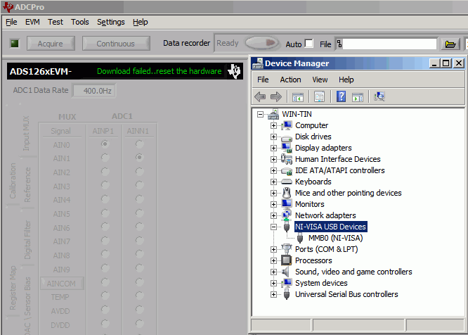 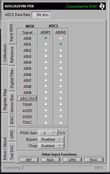
Image 15,16: ADCPro unable to detect and expected result in softwareLabView often is tricky and not very reliable in operation, as even after just ~10 minutes of fiddling with various tool settings I got it to crash with error: 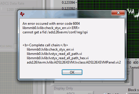 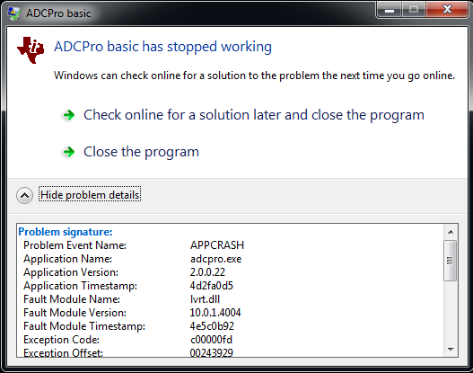
Image 17,18: Random errors and crashes in ADCProNo further operation was possible until application was closed and reopen again. Sometimes it was just hanging without any error message. Anyhow, let’s see what software allows us to do, when it works. Configuration of ADC and capturing data is simple and intuitive. For data analysis three main “tests” are available: - Data monitor – just shows counts and HEX codes.
- FFT – Plot frequency dB/dBfs FFT chart with basic AC analysis (SNR,THD,SINAD,dB power,SFDR)
- Histogram – Samples distribution histogram, with basic DC analysis (StDev,Codes(peak),Mean,ENOB,Noise free bits)
- Scope – Plots time/voltage diagram, just like oscilloscope, with FSR or Auto amplitude scale and horizontal sample count axis
Wish there could be simple version of DMM-style monitor as well to show converted voltage in big bright letters, with fast realtime single or continuous acquisition refresh setting. Given existing LabView application complexity making that plugin would be matter of few minutes. That could be handy for sensor tweaking and adjustment, as existing continuous acquisition speed is extremely slow. 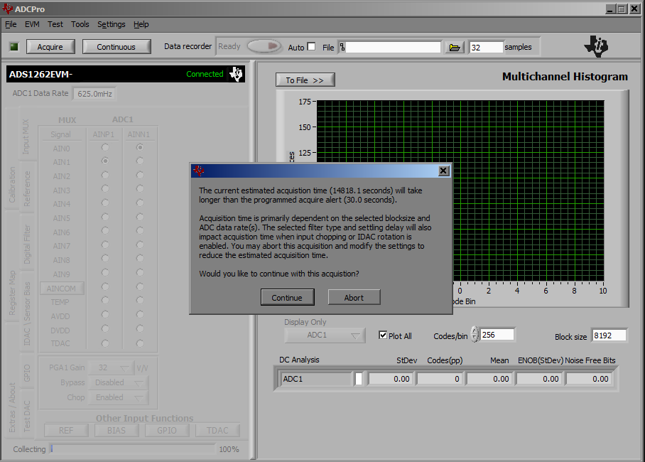
Image 19: Long sampling warning with default 30 second settingAnd for sake of old computers, ancient Windows 2000 is not supported by PDK software, throwing non-stop errors when trying to load ADS126XEVM plugin in ADCPro. I had Windows 2000 SP4 on my Tektronix scope when I tried this. Overall, would be great to have TI better release simple example software and firmware code templates for Linux & ARM environment, in GCC and Python implementations. That would help open source community to get started in no time, and also would solve beginner firmware interfacing issues of embedded ARM projects. NI LabView is not the best choice for starters. Interfacing ADCTexas Instruments ADS1262 using standard 3-wire SPI interface. This interface is easy to implement, can run up to few tens of MHz and reliable to operate. Chip select signal controls multi-device SPI bus operation, disabling ADS1262’s interface when not needed. Related signals map for digital interface is described below: ADS1262 Pin | Signal name | Function | Active type | Direction | Notes | Pin 9 | START | Start conversion input | Rising edge | Input | Tie low if SPI commands used | Pin 10 | CS | Chip select input | Low level | Input | DOUT will be in HIZ, can be tied low | Pin 11 | SCLK | SPI Clock input | Falling edge | Input | Place series resistance to reduce ringing | Pin 12 | DIN (MOSI) | SPI Data input to ADC | | Input | Place series resistance to reduce ringing | Pin 13 | DOUT/DRDY (MISO) | SPI Data output to MCU + Data ready | | Output | Place series resistance to reduce ringing | Pin 14 | DRDY | ADC Conversion ready | Falling low | Output | Goes low when ADC conversion is complete | Pin 20 | RESET/PWDN | RESET input | Active low | Input | If low >65536 Fclk ADC enters power down mode |
Table 5: Digital pins definition of ADS1262
DRDY and START signals are not required to work with ADC, but it is a good practice to use them, so MCU would not run SPI transfers and processing when data is not ready. EVM module have J1 header with both TOP (male pins) and BOTTOM (female sockets) connectors: Pin | Signal name | Direction | Description | Description | Direction | Signal name | Pin | J1.1 | NC | Reserved | Not connected | Trigger ADC conversion | Input,CTRL | START | J1.2 | J1.3 | SCLK | Input,SPI | SPI Interface clock input | Not connected | Reserved | GND | J1.4 | J1.5 | NC | Reserved | Not connected | Reset or power down in | Input | RESET/PWDN | J1.6 | J1.7 | CS | Input,SPI | SPI chip select input | Not connected | Reserved | NC | J1.8 | J1.9 | NC | Reserved | Not connected | Digital ground | Ground | GND | J1.10 | J1.11 | DIN | Input,SPI | SPI Data input, MOSI | Not connected | Reserved | NC | J1.12 | J1.13 | DOUT/DRDY | Output,SPI | SPI Data out MISO/ Ready | Not connected | Reserved | NC | J1.14 | J1.15 | DRDY | Output | Conversion complete/Ready | Serial EEPROM Clock | Bidir,I2C | SCL | J1.16 | J1.17 | NC | Reserved | Not connected | Digital ground | Ground | GND | J1.18 | J1.19 | NC | Reserved | Not connected | Serial EEPROM DATA | Bidir,I2C | SDA | J1.20 |
Table 6: Port definition J1 (both TOP/BOTTOM pins) 
Schematics 1: Interface connector J1Power to ADC or onboard regulators provided via J5 header in middle bottom side of the ADS126XEVM module: Pin | Signal name | Direction | Description | Description | Direction | Signal name | Pin | J5.1 | NC | Reserved | Not connected | Not connected | Reserved | NC | J5.2 | J5.3 | +5V input | Power in pos | +5V to AVDD or +2.5V LDO | -5V to -2.5V LDO | Power in neg | -5V | J5.4 | J5.5 | GND | Ground | Module ground | Module ground | Ground | GND | J5.6 | J5.7 | NC | Reserved | Not connected | Not connected | Reserved | NC | J5.8 | J5.9 | +3.3V input | Power in dig | +3.3V to DVDD digital | Not connected | Reserved | NC | J5.10 |
Table 7: Port definition J1 (both TOP/BOTTOM pins) 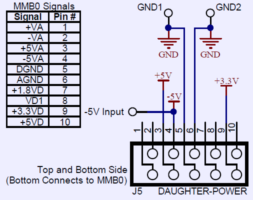
Schematics 2: Power connector J5Also it’s possible to interface ADS1262 using SPI in Python. While I did not tried this yet, it should be rather simple for any python-programmer. Setting hardware config up to work with spidev library is very fast task. Interfacing with MCUAs a test environment, generic MCU Embedded Artists’ LPCXpresso Base Board with LPC1768 module was used. MCU will be accessing ADC thru one of available SPI interfaces and communicate resulting conversions data into voltage readout math and data logs. For debug and data logging onboard USB-UART bridge and PuTTY terminal freeware program is used, with port U22 connected to PC. Hardware connections:Base board and LPC1768 LPCXpresso module are supplied with schematics, so it’s not a problem to connect all our devices together. I used SSP1 port on MCU. 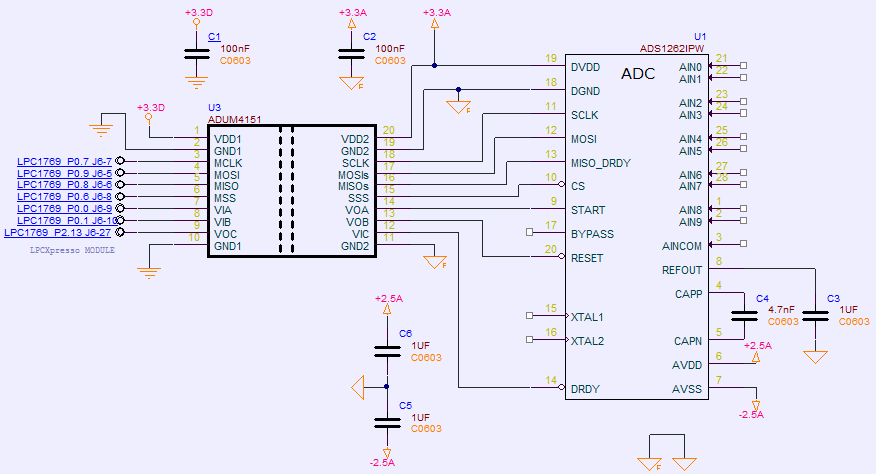
Schematics 3: MCU SPI isolation interfaceADUM4151 SPI isolator IC was used to avoid ground and power noise pickup from digital control and host PC. This will also allow to have battery powered ADC, to allow floating input signals, without risk of unwanted ground currents. Large dot-matrix vacuum-fluorescent display with 256×64 dots resolution will be used to display measurements and auxiliary data, such as ADC channel selected, reference voltage settings, gain settings and temperature in further experiments. It’s connected to MCU’s port as defined in table below MCU Port | VFD signal | P2.4 | Data bit 0 | P2.5 | Data bit 1 | P2.6 | Data bit 2 | P2.7 | Data bit 3 | P2.8 | Data bit 4 | P2.9 | Data bit 5 | P2.10 | Data bit 6 | P2.11 | Data bit 7 | P0.28 | CS | P0.27 | WR | P2.13 | CD | P2.12 | RD |
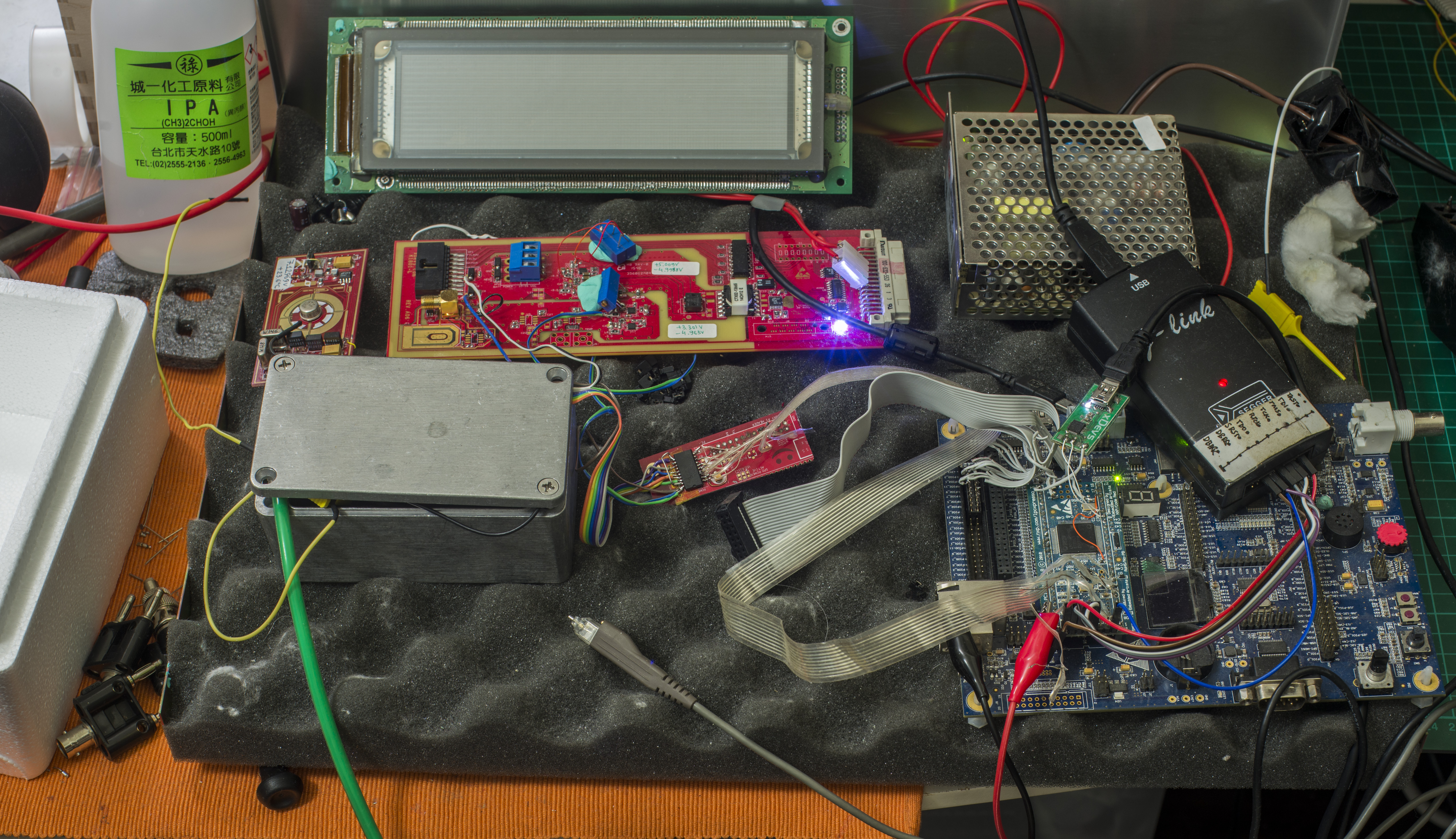
Table 8: VFD parallel interface connection to MCU Software/firmware code examples for MCU and ADS1262You can download test mercurial repository from here. It have IAR ARM v7.50 project, with everything ready for LPCXpresso LPC1769 and ADS1262EVM operation. If one not familiar with mercurial DVCS, feel free to execute git-like command: $ hg clone http://dev.xdevs.com/hg/ads1262_demo/After all connections done, first step is to write some low-level code to use MCU’s SPI interface block to write/read data into interface. Using ADS126X library taken from TI’s Reference Design with AC Bridge Excitation, we easily modify it and adopt for specific MCU (LPC1768/LPC1769): unsigned char ADS126xXferByte(unsigned char cData) { while(SSP_GetStatus(LPC_SSP1, SSP_STAT_BUSY)); // Wait for SSP1 to become free SSP_SendData(LPC_SSP1, cData); // Send byte cData while(SSP_GetStatus(LPC_SSP1, SSP_STAT_BUSY)); // Wait for SSP1 to become free return SSP_ReceiveData(LPC_SSP1); // Receive data and return}This is transfer byte function, using SSP1 hardware interface block and pins P0.6, P0.7, P0.8, P0.9. Chip select for ADC can be controlled as GPIO manually as well, with simple function: void set_adc_START(uint8_t state) { if (0 == state) ADS_START_DEASSERT; else if (1 == state) ADS_START_ASSERT; else assert(0); //Aborts program, incorrect parameter received}Macros ADS_START_ASSERT and ADS_START_DEASSERT are just wraps for CMSIS’s GPIO_SetValue and GPIO_ClearValue functions for GPIO P0.0. Rest of code is pretty much intact, taken from [adc2_demo.c, adc2_demo.h, ADS126x.c, ADS126x.h and console.c, console.h] files from TI’s demo app. I removed or deactivated ADC2 related functions and blocks, as we have ADS1262, not dual-ADC ADS1263 chip. Now, going to higher level, we need to prepare register data and initialize our ADS1262 before any data sampling can be done, like so: uint8_t AdcRegData[ADS126x_NUM_REG]; //Stores the register read valuesuint8_t WriteRegData[ADS126x_NUM_REG]; //Stores the register write valuesADS126xReadRegister(ID, ADS126x_NUM_REG, AdcRegData); //Read ALL registers/* Configure Register Settings */WriteRegData[ID] = AdcRegData[ID]; //IDWriteRegData[POWER] = (AdcRegData[POWER] & ~RST) | INTREF; //POWER (RESET = 0, INTREF = 1)WriteRegData[INTERFACE] = STATUS | CRC_ON; //INTERFACE (STATUS & CRC bytes ON)WriteRegData[MODE0] = MODE0_DEFAULT_VALUE; //MODE0 (reset to default)WriteRegData[MODE1] = AdcRegData[MODE1]; //MODE1WriteRegData[MODE2] = (AdcRegData[MODE2] & ~BYPASS) | GAIN_2; //MODE2 (BYPASS OFF, GAIN1 = 32 V/V)WriteRegData[INPMUX] = MUXP_AIN6 | MUXN_AIN7; //INPMUX (AINP1 = AIN1, AINN1 = AIN2)WriteRegData[OFCAL0] = OFCAL0_DEFAULT_VALUE; //OFCAL0 (reset to default)WriteRegData[OFCAL1] = OFCAL1_DEFAULT_VALUE; //OFCAL1 (reset to default)WriteRegData[OFCAL2] = OFCAL2_DEFAULT_VALUE; //OFCAL2 (reset to default)WriteRegData[FSCAL0] = FSCAL0_DEFAULT_VALUE; //FSCAL0 (reset to default)WriteRegData[FSCAL1] = FSCAL1_DEFAULT_VALUE; //FSCAL1 (reset to default)WriteRegData[FSCAL2] = FSCAL2_DEFAULT_VALUE; //FSCAL2 (reset to default)WriteRegData[IDACMUX] = MUX2_NO_CONM | MUX1_AINCOM; //IDACMUX (IDAC1MUX = AINCOM)WriteRegData[IDACMAG] = MAG2_OFF | MAG1_500uA; //IDACMAG (IDAC1MAG = 500 uA)WriteRegData[REFMUX] = RMUXP_AIN4 | RMUXN_AIN5; //REFMUX (REFP = AIN0, REFN = AIN3)WriteRegData[TDACP] = TDACP_DEFAULT_VALUE; //TDACP (reset to default)WriteRegData[TDACN] = TDACN_DEFAULT_VALUE; //TDACN (reset to default)WriteRegData[GPIOCON] = CON6_AIN09 | CON5_AIN08; //GPIOCON (Enable GPIOs on AIN8 & AIN9)WriteRegData[GPIODIR] = GPIOCON_DEFAULT_VALUE; //GPIODIR (reset to default)WriteRegData[GPIODAT] = DAT5_AIN08; //GPIODAT (Biases bridge with + polarity)ADS126xWriteRegister(ID, ADS126x_NUM_REG, &WriteRegData[0]); //Write ALL registersNow we can try to read 16 samples from ADC: char outString[256]; char tempString[256]; uint8_t i = 0; uint16_t ADC1count = 0 //Data conversion counters uint8_t AdcRegData[ADS126x_NUM_REG]; //Stores the register read values uint8_t WriteRegData; //Stores register write value uint8_t ADC1_Bytes[16]; set_adc_START(0); //Set START low ADS126xReadRegister(ID, ADS126x_NUM_REG, AdcRegData); //Read ALL registers WriteRegData = (AdcRegData[MODE2] & ~DR_MASK) | DR_60_SPS; //MODE2 ADS126xWriteRegister(MODE2, 1, &WriteRegData); //Configure ADC1 data rate set_adc_START(1); //Set START high while((ADC1count < MinNumADCReadings) && (ADC2count < MinNumADCReadings)) { for(i = 0; i < 16; ++i) { //Clear Data Arrays ADC1_Bytes = 0; } WaitForDRDY(); //Wait for ADC to ready data set_adc_CS(0); // Chip select active ADS126xXferByte(RDATA1); //Send RDATA1 command for(i = 0; i < 16; ++i) { ADC1_Bytes = ADS126xXferByte(0); if (ADC1_Bytes[0] & ADC1_NEW) { //ADC1 Data New? ADC1count++; } }; set_adc_CS(1); // Chip select deactive} set_adc_START(0); //Set START low strcpy(outString,\"\\r\\nADC1count = 0x\"); hex2asc(&ADC1count,4,2,tempString,1); strcat(outString,tempString); strcat(outString,\"\\r\\nADC2count = 0x\"); hex2asc(&ADC2count,4,2,tempString,1); strcat(outString,tempString); strcat(outString,\"\\r\\n\"); print2Console(outString);Our samples are now available in ADC1_Bytes variable array. Test setupAccurate testing and verification of high-resolution ADC is not a simple task. It require stable and precision instrumentation, with good low-noise performance and cross checking, to make sure artifacts or signal variations are not coming from instruments itself, but from device under test. We talking microvolts and ppm-level (0.0001%) values here, so it would not be cheap to test. Some of gear I used during experiments with this ADS1262EVM: Not everything will be used every time, so more details and connections are discussed below in specific experiments. I prepared couple of experiments with this ADC, to evaluate it’s performance and noise. This can give us idea, how much noise-free digits we can have in readings, after all conversion work done. 24-bit Σ-Δ ADCs were suitable for easy 4½,5½-digit readings, so it’s interesting to see what new 32 bit chip can offer. As comparison, same tests performed with high-performance integrating type ADC, using pair of industry standard 7½- and 8½-digit DMMs. ADCs used in these instruments provide 27/28-bit readings, are expensive, difficult to test and require many selected parts. Cost of designing such ADC easily go up in tens thousands $USD, often involving custom ASIC design and component selection. So it’s interesting to see how new $10 USD chip can compete. Of course, DMM consist of many other function blocks, which are absent on single ADC chip, but some careful cross-references still can be made. Experiment 1 : Out of the box measurementLet’s first see what ADS1262 can do, without any external devices or sensors attached. One of common conditions – is zero stability, which is often important for low-level signal measurements. As with every analog circuit, ADC front-end have some parasitic voltage and current offsets, which are visible by non-zero code even with dead ground short present on input channel pins. It’s important to have these offsets stable and constant in time, so we can deduct this error value from our reading, using simple math in software. Zero stability and noiseWith minimum amount of external gear we can do quick testing of zero voltage stability, noise and offsets. This is done by soldering copper short wire to ground directly at ADS1262 AIN pins and module ground. 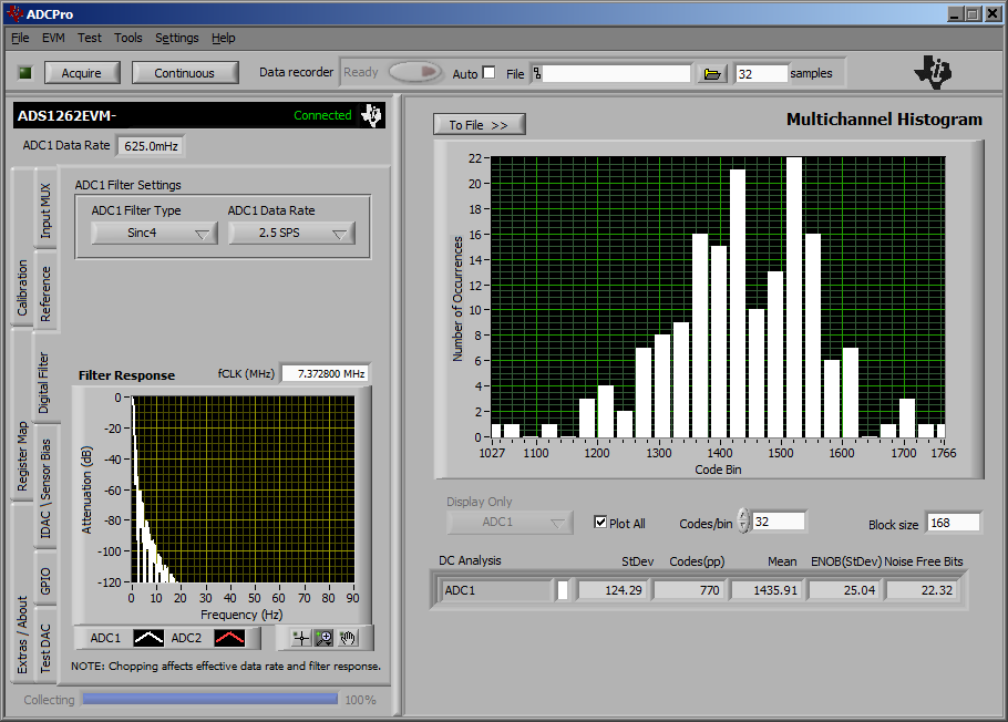
Image 20: Zero noise performance with MMB0 connected and LabView PDKWith MMB0 and bundled LabView software, ADC with zero at input able to reach 25 bits of ENOB, with 22 noise free bits. This is good result, providing better data than 24-bit ADC could do, so less noisy readings can be takes even with such a basic setup. 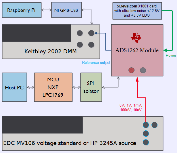
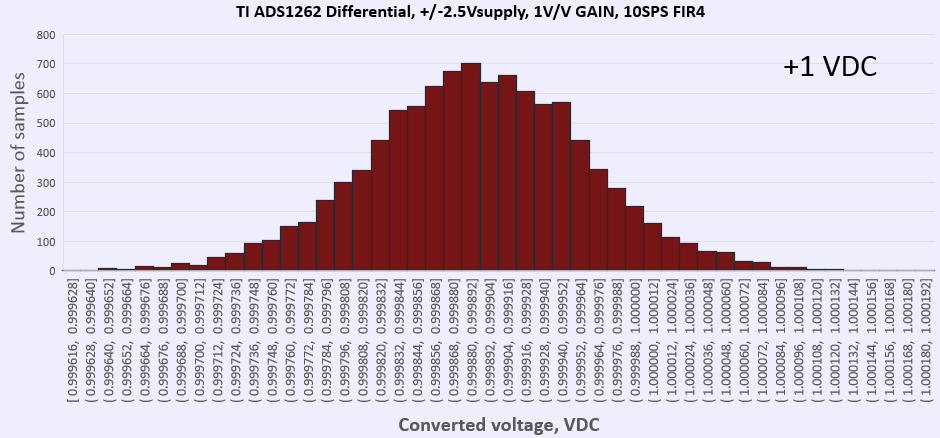
Image 21: Experiment 1 connections and setupHere are some low level DC voltage signal measurements, still using EVM kit without any additional modifications or shielding. Results are listed on graphs below. X-axis marks are seconds, blue chart on Y-axis is measured value (VDC). Additional red scale on right side shows ppm deviation. (0.1% being equal 1000ppm) Voltage source is EDC MV106 DC voltage standard, which is stable to ~5ppm. No input divider or attenuation used. First test, 1VDC input, PGA gain set to 2. 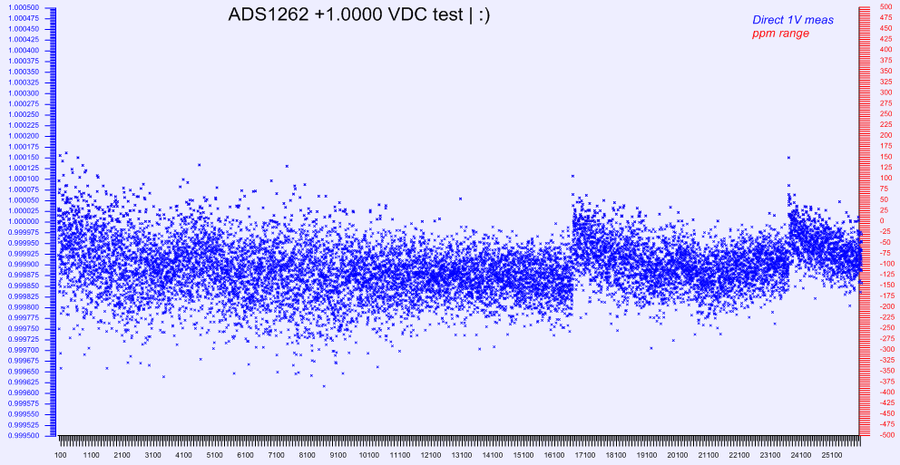
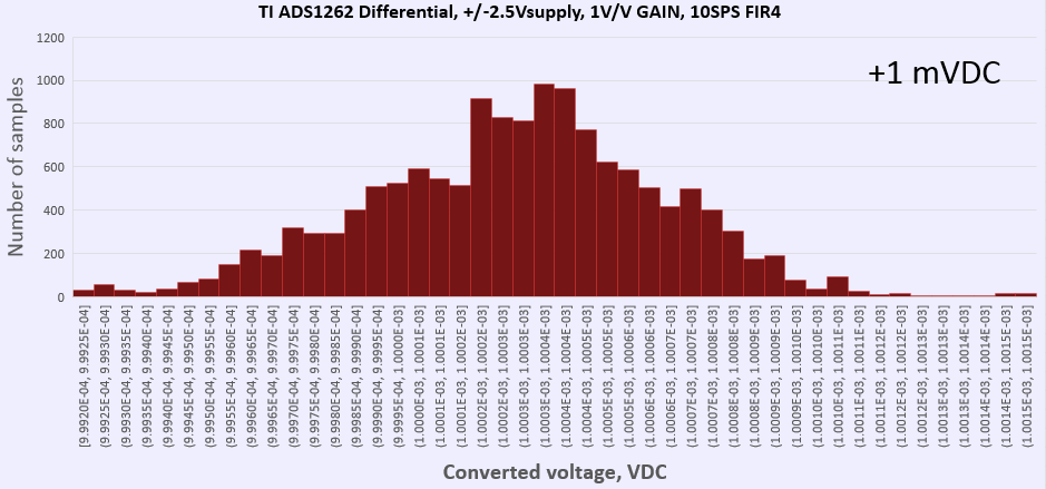
Image 22: +1VDC voltage chartThere is some signal scatter on the first section of the graph, indicating stray airflows over EVM board. After placing module in plastic box, readings became more stable (can see this from 12K seconds in middle). Few times wires were fiddled around, causing jumps at 17100 and 24100 seconds. Overall graph span is 7.2 hours, with readings window within 150ppm. With just simple moving average or median filtering this will let us to have stable 5½ digit measurements. Second test, lower voltage, 1 mVDC, PGA gain set to 8. Graph scale is in millivolts. 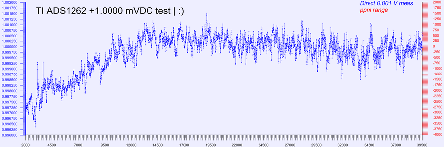
Image 23: +0.001VDC voltage chartThings are bit worse with 1000 times less voltage signal. First 10000 seconds some setting was happening, due temperature change around circuit. Further readings remained stable within 1500ppm corridor. This is still able to give us nice 5½-digit readings, with 1mV level signal. Most of handheld DMMs have this as least significant digit. Now even lower, 100μVDC with PGA set to 16. Graph scale is in millivolts. 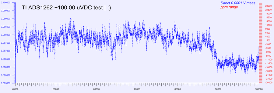
Image 24: +0.0001VDC voltage chartGoing even lower, to 100μV things get bit off, and results urge for calibration. But even without calibration, using integrated reference, our readings dropped to 98 μV average. Readings drop after 90K seconds are due to cable position change. Triboelectic effects, thermal EMFs and shielding become important down at microvolts. And lowest signal, 10μVDC, right down to noise, with PGA set to 32. Graph scale is in millivolts. 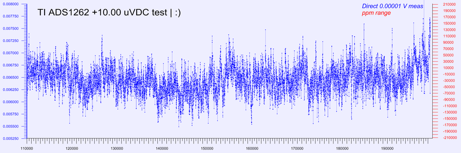
Image 25: +0.00001VDC voltage chartAt mere 10 μVDC result was 6.5μV average, which is too much of an error. It is now difficult to be sure, if it’s input signal have noise, or ADC itself with PGA contribute error into conversion data. Just indication, how hard it can be to measure something at 10μV. Device under test | Input signal | Setting | CSV-datalog | Histogram | Std.Dev | RMS value | TI ADS1262 ADC | +10 μVDC | AIN0,AIN1 Differential, 2.5SPS FIR4, CHOP ON | | | 2.67788E-7 | 2.80775E-9 | TI ADS1262 ADC | +100 μVDC | AIN0,AIN1 Differential, 2.5SPS FIR4, CHOP ON | | | 4.00219E-7 | 6.28593E-9 | TI ADS1262 ADC | +1 mVDC | AIN0,AIN1 Differential, 2.5SPS FIR4, CHOP ON | | | 4.23272E-7 | 5.24112E-9 | TI ADS1262 ADC | +1 VDC | AIN0,AIN1 Differential, 2.5SPS FIR4, CHOP ON | | | 6.18829E-5 | 9.96740E-5 |
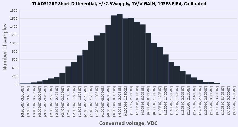
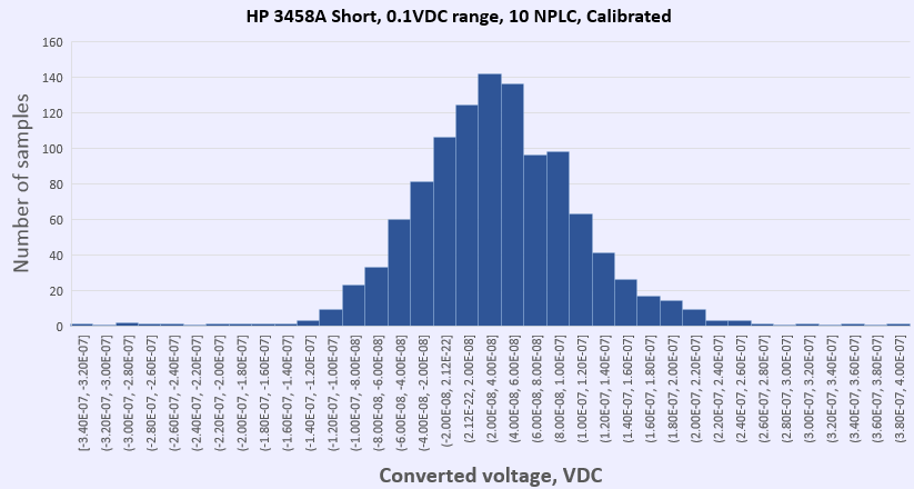
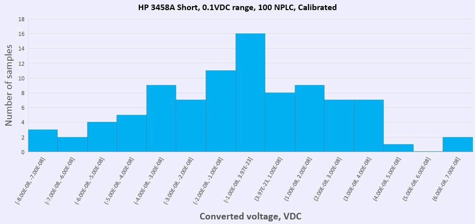
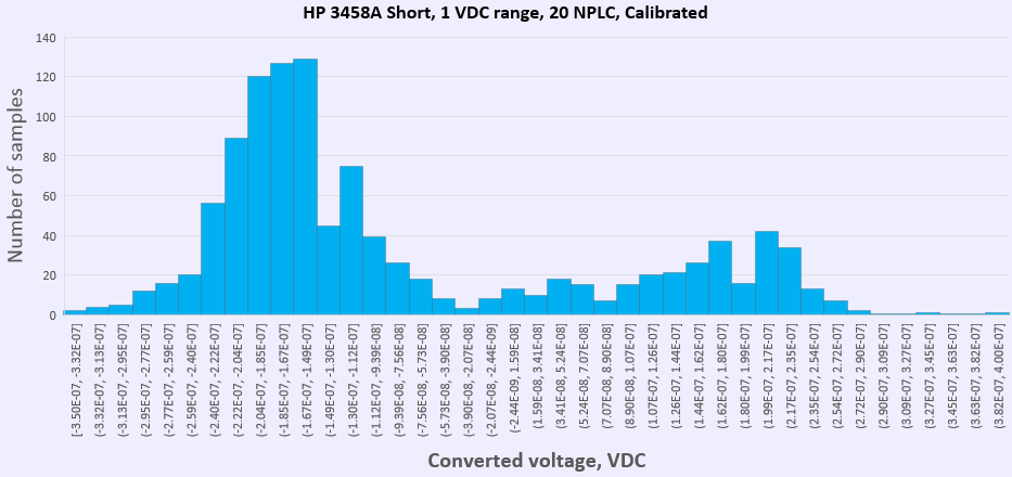
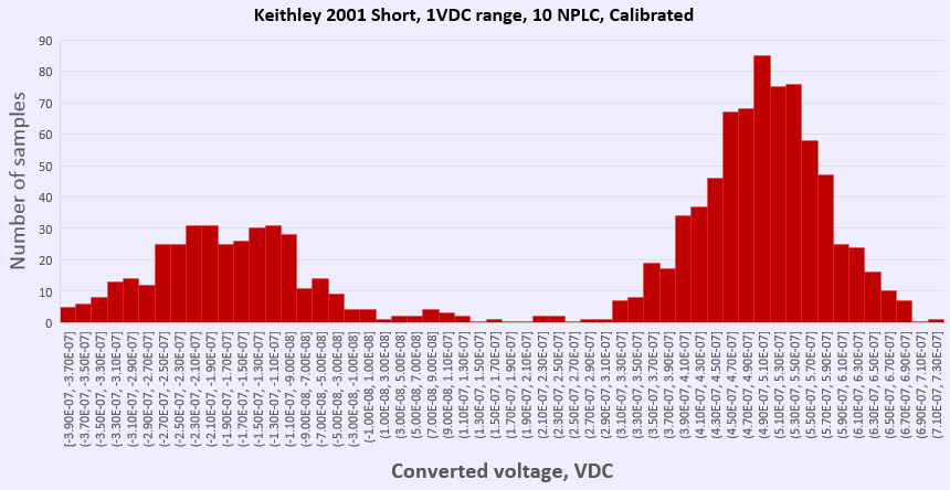
Table 9: Low-voltage signals test results Overall, I’m impressed, even with 1mV signal we can get 5½-digit readings without a single extra penny spent on parts or any amplifiers. Zero input performanceNow time to test zero input performance. This will tell us how noisy is ADC itself, removing errors from reference or input signal instability. Output code is taken at two different gains, A=1 and A=32 and sampling speeds 10 SPS and 2 SPS to evaluate noise performance. Zero voltage test with inputs shorted also tested on 8½-digit Keithley 2002 and 8½-digit HP 3458A DMMs to give comparison with state-of-art integrating ADC performance. This time only ADC module is used, and located in metal can for good shielding and to avoid possible airflow. This is important, as even little 0.1°C temperature gradient over PCB can cause thermal voltages in hundreds of microvolts. PCB and component pins are forming many thermocouples across signal path, due to difference in used metals. 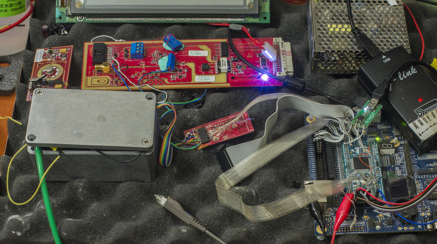
Image 26: Zero measurement setupSummary table with test setups and results involved in this experiment: Device under test | Input signal | Setting | CSV-datalog | Histogram | Std.Dev | RMS value | TI ADS1262 ADC | Zero, input shorted | AIN0,AIN1 Differential | | | +1.13049E-7 | +3.02082E-10 | TI ADS1262 ADC | ±Gain=32, CHOP ON | AIN0,AIN1 Differential | | | 3.68621E-9 | 8.20724E-15 | HP 3458A DMM | Zero, input shorted | Range 100mV, NPLC10, 5Hz, AZ ON | | | +7.2252E-8 | +5.93032E-12 | HP 3458A DMM | Zero, input shorted | Range 100mV, NPLC50, AZ ON | | | 3.34488E-8 | 1.17252E-12 | HP 3458A DMM | Zero, input shorted | Range 100mV, NPLC100, AZ ON | | | 3.16788E-8 | 8.93156E-14 | HP 3458A DMM | Zero, input shorted | Range 1V, NPLC20, 2.5Hz, AZ ON | | | 1.35463E-7 | 4.56924E-11 | Keithley 2002 DMM | Zero, input shorted | Range 1V, NPLC10, 5Hz, AZ ON | | | 2.12681E-7 | 1.14349E-10 | Keithley 2001 DMM | Zero, input shorted | Range 1V, NPLC10, 5Hz, AZ ON | | | 3.30339E-7 | 2.75974E-10 |
Table 10: Zero short noise test results Zero noise performance puts ADS1262 into close proximity with expensive 7½-digit DMM, so with good front-end design and attenuation, it is possible to design and build very good measuring system, with 6½-digit stable scale resolution. With some bits of smart math and filtering even 7½-digit values should be within reach. Integrated PGA does not contribute much noise, and with calibration it allow to measure low amplitude signals, saving a lot of trouble on front end design, which before often had use of very expensive resistors and careful precision operational amplifier design, like we can see in HP 3458A or Keithley 2002. And only special-purpose instruments, such as nanovoltmeters can go voltage ranges below 100mV, where ADS1262 can actually offer better noise and accuracy performance than low voltage 100mV range of even 8½-digit HP 3458A (which cost more than USD $9700 new!). Experiment 2 : Testing internal referenceBecause ADS1262’s voltage reference is accessible from external pin, we can connect precision DMM and monitor stability of this voltage reference output. This can help us to evaluate temperature dependence and overall impact on absolute accuracy from internal reference. HP 3458A, Keithley 2510 and DIY thermal chamber was used for this experiment. Knowing how stable internal reference is, designer can decide if better reference is required in specific application, or internal source is stable enough (for example, in case of ratiometric measurements between two signals, where only short-term stability is important). Internal reference temperature stability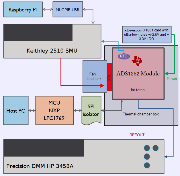
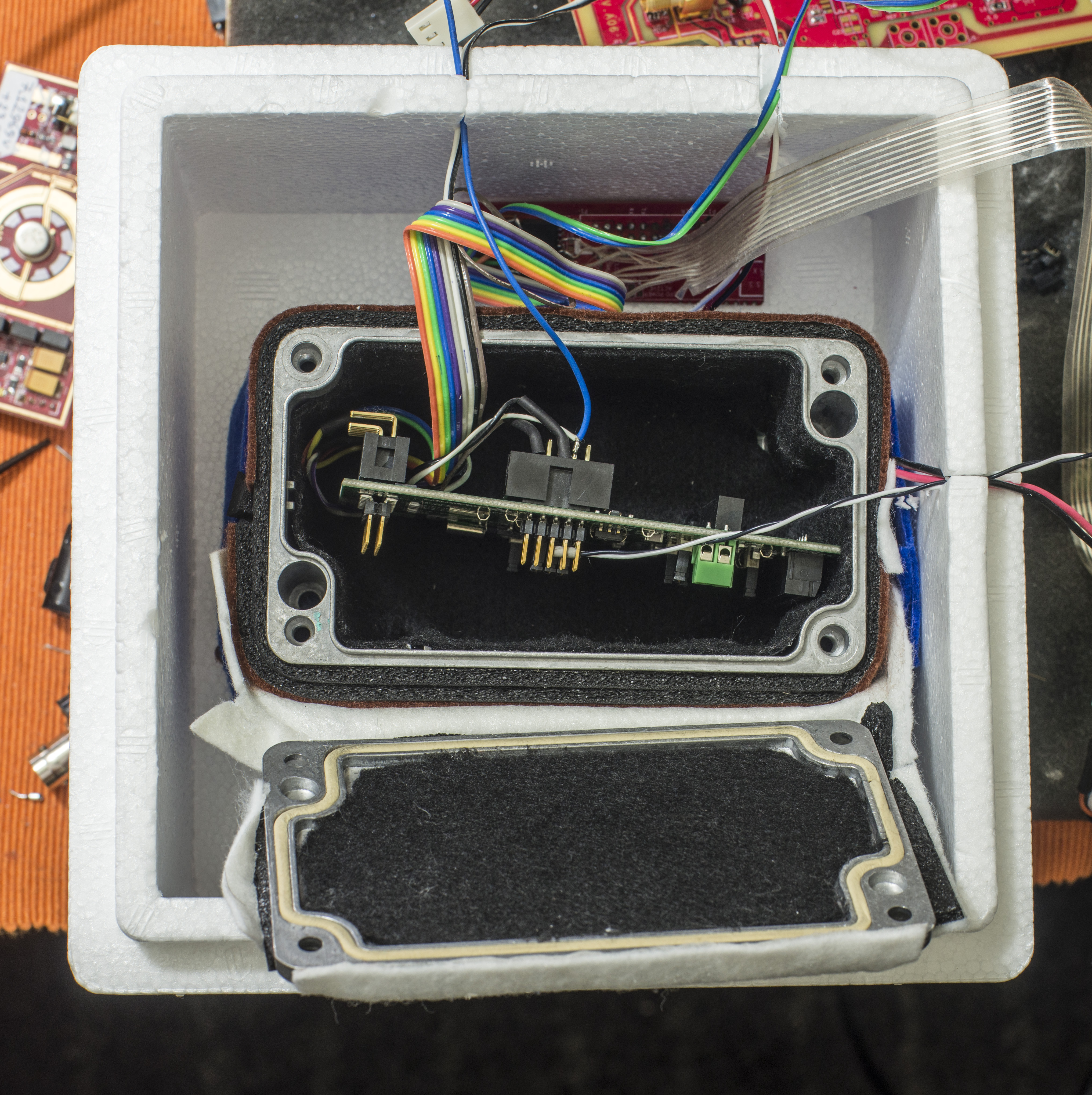
Image 27: Measurement setup for experiment 2This experiment will help us to check actual reference voltage deviation, from variance of ambient temperature. Block diagram of this test setup is as below: - EVM located in foam chamber box to allow control over ambient temperature
- TEC module with heatsink and small fan located in chamber box
- TEC SMU controlling temperature in chamber box from +20°C to +65°C using Honeywell HEL-705 platinum RTD as sensor
- HP 3458A DMM measuring REFOUT internal reference from ADS1262, using GPIB pod and Raspberry Pi
- ADS1262 measuring it’s own temperature sensor using internal reference
Initial data without controlled box temperature, over 20-hour test period: 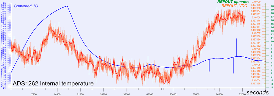
Image 28: Initial temperature stability chart, no temperature controlBlue line on graph is internal ADS1262 temperature, measured by chip itself, and orange are REFOUT output measurement by Keithley 2002 DMM. Extra scale, marked in green indicate μV/V deviation of reference voltage. 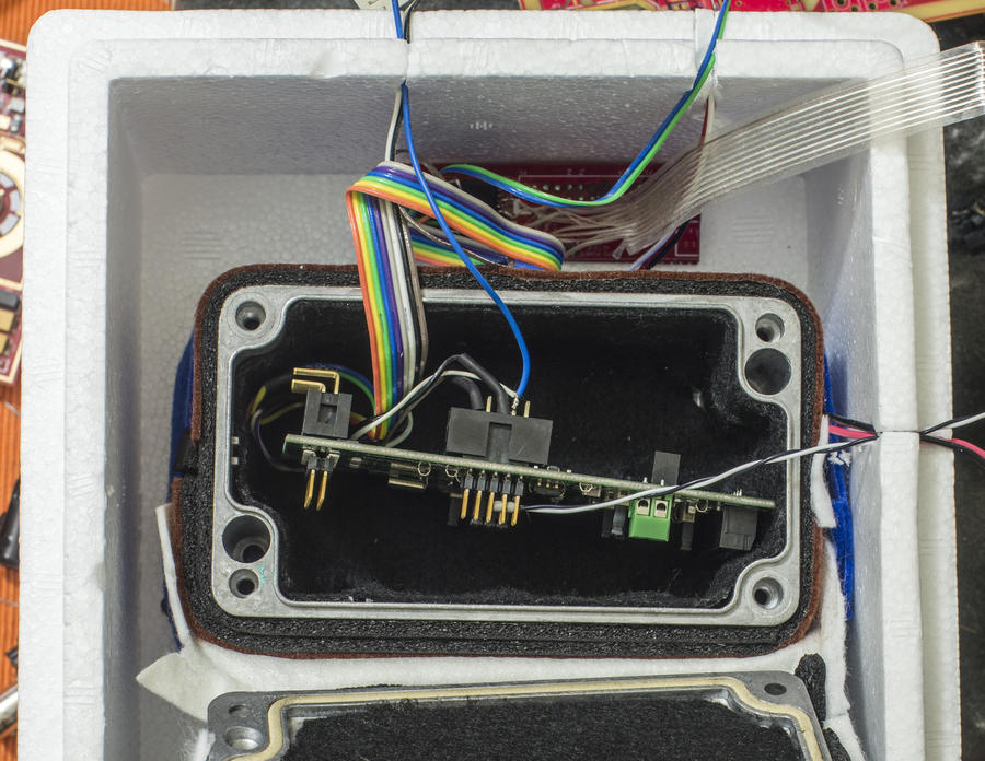
Image 29: Simple DIY temperature chamberNow I will use Keithley 2510 TEC SourceMeter to control temperature inside Styrofoam box with ADC module. Module itself is in same cast metal box, but this time with 40W TEC mounted on it’s bottom. Another side of TEC is attached to small fansink with +5V DC fan. Temperature sensor for feedback is fixed on ADS1262 pin header, to provide good thermal coupling. This is ultimately will be the point, to which SMU will try to maintain chamber temperature. 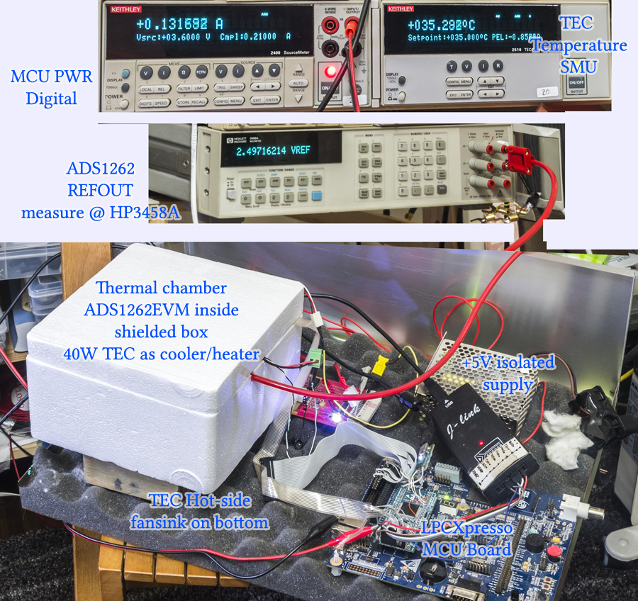
Image 30: Test for experiment 2 in progressExpected stability of internal reference voltage to be less than 6 ppm/K, with hysteresis no more than 50 ppm. Effect of changing reference voltage and ADC temperature changes can be measured as well, by using ADC to sample known stable DC voltage signal. Or in this case, reference output REFOUT was measured using external precision DMM (which is tested to be stable better than 1 ppm/day), while ADC was configured to measure it’s own temperature. 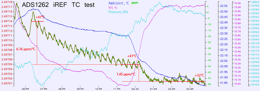
Image 31: Initial temperature coefficient test with temperature ramp downInitial reference voltage changed with rate 6.16 ppm/°C, but later temperature change from +41°C to +32°C observed much better rate 1.45ppm/°C. Sawtooth-type variation of reference voltage indicate better shielding attention requirement, as TEC is pumped with ~20W of power each time, coupling noise into ADS and circuits around. If absolute accuracy and stability is first priority, thermally stabilized reference sources like Linear LM399 or Linear LTZ1000 can be used. Both of these provide very stable ~7VDC, and some attenuation circuit would be required to bring reference voltage down to ADS1262 levels. Example of such circuit is shown on schematics below: 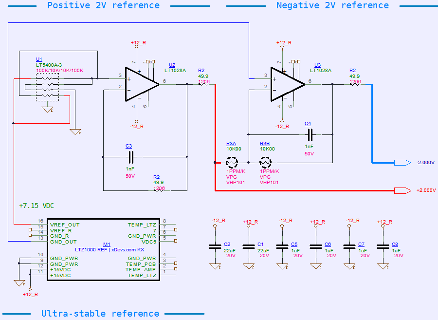
Schematics 4: ± 2 VDC ultra-stable voltage referenceModule M1, based on ultra-zener LTZ1000 provides stable +7 VDC which can have long-term stability about 1 ppm/year. This voltage is accurately divided by U1 resistor network (Linear LT5400A-3, matched to 0.01% with 0.2ppm/K matching TCR, long-term stability <2ppm/2khr). This brings voltage down to 2 VDC, which is buffered by U2 low-noise opamp. Precision metal foil resistor network R3 and opamp U3 providing inverted -2 VDC output. This circuit provides ±2VDC reference suitable to drive ADS1262. It is crucial to use stable resistors in this circuit, as ultimately main contribution of error would be from resistors, not the active parts. ADC system with this external reference can have great accuracy, which would be limited by ADS1262 ADC stability. Initial calibration for exact voltage levels would be also required, as LTZ1000 have absolute accuracy only 1%. We will build this circuit and have some experiments and measurements with it on follow-up Part 2 article. Conclusion, kit scoring and verdictMany readers may say, why spend so much effort in testing, while specifications of TI ADS1262 are already very good? Well, one of purposes why I applied this EVM kit and ADS1262 is to build portable precision null-meter, to compare various voltage references and DC standards. High-end expensive 8½-digit DMMs like HP 3458A or Keithley 2002 are not usually available for many engineers. EE hobbyists mostly do have more popular 6½-digit bench DMMs, such as Keithley 2000, HP/Agilent/Keysight 34401A or similar Rigol, Fluke DMMs. These engineers rarely have equipment required to accurately calibrate or even test these meters, leave alone comparing DC voltage/current standards with high enough accuracy. Building accurate null-meter based on 32-bit low-noise ADS1262 is one of practical tasks which would really benefit from external stable voltage reference, as this means that calibration would be required only once during initial assembly and test. Then such kit can be sent to different people, with high confidence in accuracy and results. In a way, it can be used as voltage transfer tool between different instruments. More details on practice to be covered in next second part article, which is coming soon. EVM Features and constructionAssembly quality is top notch, as expected from reference design. All parts are easily accessible for soldering and probing. No BGA or CSP packages used. EVM kit in review allowed us to demo few aspects of long-scale ADC and prototype few ideas. Use and connections to ADS1262 EVM were easy even for beginners. Solid A mark on performance. PerformanceWith given test results, TI ADS1262, as one of 32-bit all-in-one ADC products, there is nothing to complain about. Using simple SPI interfacing and control, it was possible to create very nice 5½-digit capable measurement setup. This brings unheard level of resolution into relatively low-cost measurement applications and more new possibilities in instrumentation performance. With proper design care, good power supply and decent input attenuation design, it is not hard to achieve even better performance. Bundled software examplesProvided software examples are rather unfriendly, especially for not experienced engineer. It’s not obvious path to locate C source-code examples for ADS126x ADC, which is hidden in another validation kit, TIPD188, not the ADS1262EVM-PDK. Lack of support with modern popular platforms, such as Raspberry Pi may require extra time to get all toolkit set and ready with ADS1262. Hopefully this article can help to fill the present void. Taking a half-point back here, A-. Bundled LabView ADCPro application is not really usable. Software supplied with reference evaluation platform must be ready to work right from the box, no exceptions. If there is reference software with EVM, it should work on usual embedded development machine, which can have common versions of LabView, python and GCC environments already installed. If it does not work at all, or break other tools operation, it’s a problem. It could be better not to include any pre-compiled software at all, only source project and templates. In that case user would use his own programs to talk with hardware, hence simple SPI interface is not a problem even for beginners. But instead of testing actual ADC performance and features, in my case I wasted whole day and had to debug this LabView connection issues on 4 different computers, and broke my existing development LabView environment just to get TI ADCPro functional. Quick search online reveals also number of other users on TI E2E forums, having similar issues with ADCPro. Firmware and MCU library is somewhat hidden too in another EVM kit documentation, not the EVM in review. Some of code pieces, like definitions for ADS1262 and functions (e.g. ADS126xREADandWRITE, ADS126xShutdown, ADS126xWake) are not implemented in library. Feels like bit beta-code condition. So overall verdict on software and examples – solid point lost right here, no questions asked. B. Price pointEVM kit is designed with support of various analog plugins and modules, allowing use of same programming environment across different ADCs/DACs. The only con is the fact that MMB0 baseboard and ADC module itself come in single package, making up for $200 USD price tag, which seems a bit too high. There are no precision sensors or external references included, which could justify that cost better. If user can have option of buying ADS126XEVM module separately from MMB0, that would save the cost issue, as not always USB-based interface board with DSP is required. That applies also to engineers who already have other TI EVMs, which may included MMB0. Also software examples primarily based on LabView, which starts at USD $999 for limited base package version. Would love to see more open software examples/templates, even plain C/Python code would do the job well. So taking a half-point off here for hidden cost, which results mark A-. Total scoreFeatures : A (100%)
Performance : A (100%)
Software : B (50%)
Pricing : A- (75%) Anyone who is looking into using new 32-bit ADC chips, and not mind writing some lines of C/Python code can choose ADS1262EVM-PDK. It would be a good choice as evaluation platform. While price might be a considering factor, decent PCB with power supplies and interfacing connectors offered, eliminating need of hardware prototyping and soldering. For system designers which plan to use ADS1262 or ADS1263 in their design, it might be easier to get chip itself and design in directly into product or prototyping board. TSSOP package used for these ADCs is not that hard to solder with usual iron, and there is need to write own firmware/software code anyway, unless you really have a LabView professional nearby on standby, to reuse TI’s libraries for every specific application. Literature
来源: 32位ADC芯片ADS1262性能测试 |


 发表于 2021-11-6 13:44:44


 发表于 2022-8-7 11:05:21

